A printable, sensor-laden ‘skin’ for robots (or an airplane)
March 24, 2017

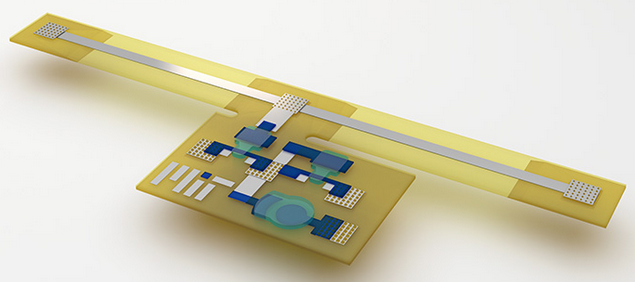
Illustration of 3D-printed sensory composite (credit: Subramanian Sundaram)
MIT researchers have designed a radical new method of creating flexible, printable electronics that combine sensors and processing circuitry.
Covering a robot — or an airplane or a bridge, for example — with sensors will require a technology that is both flexible and cost-effective to manufacture in bulk. To demonstrate the feasibility of their new method, the researchers at MIT’s Computer Science and Artificial Intelligence Laboratory have designed and built a 3D-printed device that responds to mechanical stresses by changing the color of a spot on its surface.
Sensorimotor pathways
“In nature, networks of sensors and interconnects [such as the human nervous system] are called sensorimotor pathways,” says Subramanian Sundaram, an MIT graduate student in electrical engineering and computer science (EECS), who led the project. “We were trying to see whether we could replicate sensorimotor pathways inside a 3-D-printed object. So we considered the simplest organism we could find” — the golden tortoise beetle, or “goldbug,” an insect whose exterior usually appears golden but turns reddish orange if the insect is poked or prodded, that is, mechanically stressed.
The researchers present their new design in the latest issue of the journal Advanced Materials Technologies.
The key innovation was to 3D-print directly on the plastic substrate (support structure) instead of placing components on top. That greatly increases the range of devices that can be created; a printed substrate could consist of many materials, interlocked in intricate but regular patterns, which broadens the range of functional materials that printable electronics can use.*
Printed substrates also open the possibility of devices that, although printed as flat sheets, can fold themselves up into more complex, three-dimensional shapes. Printable robots that spontaneously self-assemble when heated, for instance (see “Self-assembling printable robotic components“), are a topic of ongoing research at the CSAIL Distributed Robotics Laboratory, led by Daniela Rus, the Andrew and Erna Viterbi Professor of Electrical Engineering and Computer Science at MIT.
3D-printed sensory composite

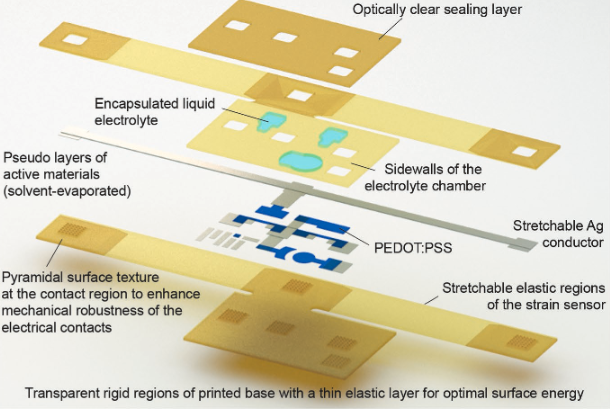
The sensory composite is grouped into 4 sets of functional layers: a base with spatially varying mechanical stiffness and surface energy, electrical materials, electrolyte, and capping layers. All these materials are 3D-printed. (credit: Subramanian Sundaram et al./ Advanced Materials Technologies)
The MIT researchers’ new device is approximately T-shaped, but with a wide, squat base and an elongated crossbar. The crossbar is made from an elastic plastic, with a strip of silver running its length; in the researchers’ experiments, electrodes were connected to the crossbar’s ends. The base of the T is made from a more rigid plastic. It includes two printed transistors and what the researchers call a “pixel,” a circle of semiconducting polymer whose color changes when the crossbars stretch, modifying the electrical resistance of the silver strip.**
A transistor consists of semiconductor channel on top of which sits a “gate,” a metal wire that, when charged, generates an electric field that switches the semiconductor between its electrically conductive and nonconductive states. In a standard transistor, there’s an insulator between the gate and the semiconductor, to prevent the gate current from leaking into the semiconductor channel.
The transistors in the MIT researchers’ device instead separate the gate and the semiconductor with an electrolyte — a layer of water containing potassium chloride mixed with glycerol. Charging the gate drives potassium ions into the semiconductor, changing its conductivity.***

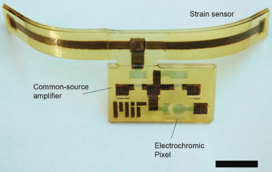
Photograph of the fully 3D-printed sensory composite shows a strain sensor (top) linked to an electrical amplifier that modulates the transparency of the electrochromic pixel (scale bar is 10mm). (credit: Subramanian Sundaram et al./ Advanced Materials Technologies)
“I am very impressed with both the concept and the realization of the system,” says Hagen Klauk, who leads the Organic Electronic Research Group at the Max Planck Institute for Solid State Research, in Stuttgart, Germany. “The approach of printing an entire optoelectronic system — including the substrate and all the components — by depositing all the materials, including solids and liquids, by 3-D printing is certainly novel, interesting, and useful, and the demonstration of the functional system confirms that the approach is also doable. By fabricating the substrate on the fly, the approach is particularly useful for improvised manufacturing environments where dedicated substrate materials may not be available.”
The work was supported by the DARPA SIMPLEX program through SPAWAR.
* To build the device, the researchers used the MultiFab, a custom 3-D printer developed MIT. The MultiFab already included two different “print heads,” one for emitting hot materials and one for cool, and an array of ultraviolet light-emitting diodes. Using ultraviolet radiation to “cure” fluids deposited by the print heads produces the device’s substrate.
** Sundaram added a copper-and-ceramic heater, which was necessary to deposit the semiconducting plastic: The plastic is suspended in a fluid that’s sprayed onto the device surface, and the heater evaporates the fluid, leaving behind a layer of plastic only 200 nanometers thick. The layer of saltwater lowers the device’s operational voltage, so that it can be powered with an ordinary 1.5-volt battery.
*** But it does render the device less durable. “I think we can probably get it to work stably for two months, maybe,” Sundaram says. “One option is to replace that liquid with something between a solid and a liquid, like a hydrogel, perhaps. But that’s something we would work on later. This is an initial demonstration.”
Abstract of 3D-Printed Autonomous Sensory Composites
A method for 3D-printing autonomous sensory composites requiring no external processing is presented. The composite operates at 1.5 V, locally performs active signal transduction with embedded electrical gain, and responds to stimuli, reversibly transducing mechanical strain into a transparency change. Digital assembly of spatially tailored solids and thin films, with encapsulated liquids, provides a route for realizing complex autonomous systems.
