Beyond LEDs: brighter, new energy-saving flat-panel lights based on carbon nanotubes
October 20, 2014

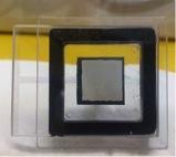
This image shows a planar light source device from the front. (Credit: N.Shimoi/Tohoku University)
Scientists from Tohoku University in Japan have developed a new type of energy-efficient flat light source, based on carbon nanotubes, with very low power consumption of around 0.1 Watt-hours of operation — about a hundred times lower than that of an LED.
In the journal Review of Scientific Instruments, the researchers detail the fabrication and optimization of the device, which is based on a phosphor screen and single-walled carbon nanotubes as electrodes in a diode structure.
Think of it as a field of conventional light-bulb tungsten filaments shrunk to microscopic proportions.
They assembled the device from a mixture liquid containing highly crystalline single-walled carbon nanotubes dispersed in an organic solvent mixed with a soap-like chemical known as a surfactant. Then they “painted” the mixture onto the positive electrode or cathode, and scratched the surface with sandpaper to form a light panel capable of producing a large, stable and homogenous emission current with low energy consumption.
“Our simple diode panel could obtain high brightness efficiency of 60 Lumens per Watt, which holds excellent potential for a lighting device with low power consumption,” said Norihiro Shimoi, the lead researcher and an associate professor of environmental studies at the Tohoku University.

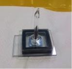
This image shows a planar light source device from the rear. (Credit: N.Shimoi/Tohoku University)
Brightness efficiency tells people how much light is being produced by a lighting source when consuming a unit amount of electric power, which is an important index to compare the energy-efficiency of different lighting devices, Shimoi said. For instance, LEDs can produce 100s Lumens per Watt and OLEDs (organic LEDs) around 40.
The new devices have luminescence systems that function like cathode ray tubes, with carbon nanotubes acting as cathodes, and a phosphor screen in a vacuum cavity acting as the anode.
Under a strong electric field, the cathode emits tight, high-speed beams of electrons through its sharp nanotube tips — a phenomenon called field emission. The electrons then fly through the vacuum in the cavity, and hit the phosphor screen into glowing.
“We have found that a cathode with highly crystalline single-walled carbon nanotubes and an anode with the improved phosphor screen in our diode structure obtained no flicker field emission current and good brightness homogeneity,” Shimoi said.

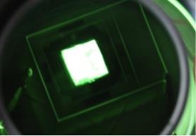
This is a plane-lighting homogeneity image of a planar light source device through a neutral density filter. (Credit: N.Shimoi/Tohoku University)
Field emission electron sources can provide intense electron beams that are about a thousand times denser than conventional thermionic cathodes (like filaments in an incandescent light bulb). That means field emission sources require much less power to operate and produce a much more directional and easily controllable stream of electrons.
In recent years, carbon nanotubes have emerged as a promising material of electron field emitters, owing to their nanoscale needle shape and extraordinary properties of chemical stability, thermal conductivity, and mechanical strength.
Highly crystalline single-walled carbon nanotubes (HCSWCNT) have nearly zero defects in the carbon network on the surface, Shimoi explained. “The resistance of cathode electrode with highly crystalline single-walled carbon nanotube is very low. Thus, the new flat-panel device has smaller energy loss compared to other current lighting devices, which can be used to make energy-efficient cathodes with low power consumption.”
“Many researchers have attempted to construct light sources with carbon nanotubes as field emitter,” Shimoi said. “But nobody has developed an equivalent and simpler lighting device.”
Abstract of Plannar light source using a phosphor screen with single-walled carbon nanotubes as field emitters
We developed and successfully fabricated a plannar light source device using a phosphorscreen with single-walled carbon nanotubes (SWCNTs) as field emitters in a simple diode structure composed of the cathode containing the highly purified and crystalline SWCNTsdispersed into an organic In2O3–SnO2 precursor solution and a non-ionic surfactant. Thecathode was activated by scratching process with sandpaper to obtain a large field emissioncurrent with low power consumption. The nicks by scratching were treated with Fourier analysis to determine the periodicity of the surface morphology and designed with controlling the count number of sandpapers. The anode, on the other hand, was made with phosphor deliberately optimized by coverage of ITO nanoparticles and assembled together with the cathode by the new stable assembling process resulting to stand-alone flat plane-emission panel. The device in a diode structure has a low driving voltage and good brightness homogeneity in that plane. Furthermore, field emission current fluctuation, which is an important factor in comparing luminance devices too, has a good stability in a simple diode panel. The flat plane-emission device employing the highly purified and crystalline SWCNTs has the potential to provide a new approach to lighting in our life style.
