Conductive ink for drawing circuits for flexible electronic books, displays, wearables
January 10, 2014

A picture drawn with conductive ink lights up a green LED (credit: American Chemical Society)
Chinese researchers have developed a novel conductive metal ink made of copper nanosheets that can be used in a pen to draw a functioning, flexible electric circuit on regular printer paper.
This development could be a step beyond the inkjet-printed circuits that KurzweilAI previously reported. The new process could pave the way for a wide range of new bendable gadgets, such as electronic books that look and feel more like traditional paperbacks, roll-up tablets, and wearables, according to the researchers.

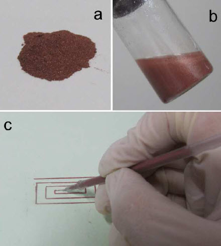
(a) Optical image of Cu nanosheet powder; (b) Optical image of Cu nanosheet ink; (c) Optical image of conductive pen. (Credit: American Chemical Society)
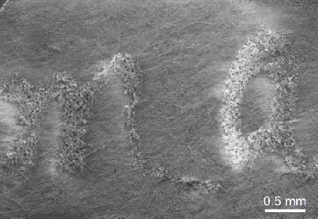
They made copper nanosheets in the laboratory, coated with silver nanoparticles to help the copper nanosheets overlap and stack together in a laminar (multi-layer) structure to improve conductivity. They then incorporated this material into an ink pen, using it to draw patterns of lines, words and even flowers on regular printer paper.
To show that the ink could conduct electricity, the scientists added small LED chips (lights) to the drawing that lit up when the circuit was connected to a battery. To test the ink’s flexibility, they folded the papers 1,000 times, even crumpling them up, and showed that the ink maintained 80 to 90 percent of its conductivity.
Wenjun Dong, Ge Wang and colleagues note that current efforts to create flexible circuits are “complicated, time-consuming, and expensive processes.”
The research was funded by the National Natural Science Foundation of China, the Zhejiang Provincial Natural Science Foundation of China, the National High-Tech R&D Program of China, the Program for New Century Excellent Talents in University, and the Program for Changjiang Scholars and Innovative Research Team in University.
Abstract of ACS Applied Materials & Interfaces paper
Large-area Cu nanosheets are synthesized by a strategy of Cu nanocrystal self-assembly, and then aqueous conductive Cu nanosheet ink is successfully prepared for direct writing on the conductive circuits of flexible electronics. The Cu nanocrystals, as building blocks, self-assemble along the 111
direction and grow into large-area nanosheets approximately 30–100 μm in diameter and a few hundred nanometers in thickness. The laminar stackable patterns of the Cu nanosheet circuits increase the contact area of the Cu nanosheets and improve the stability of the conductor under stress, the result being that the Cu nanosheet circuits display excellent conductive performance during repeated folding and unfolding. Moreover, heterostructures of Ag nanoparticle-coated Cu nanosheets are created to improve the thermal stability of the nanosheet circuits at high temperatures.


