How to change the crystal structure of graphene from metal to semiconductor
May 6, 2014

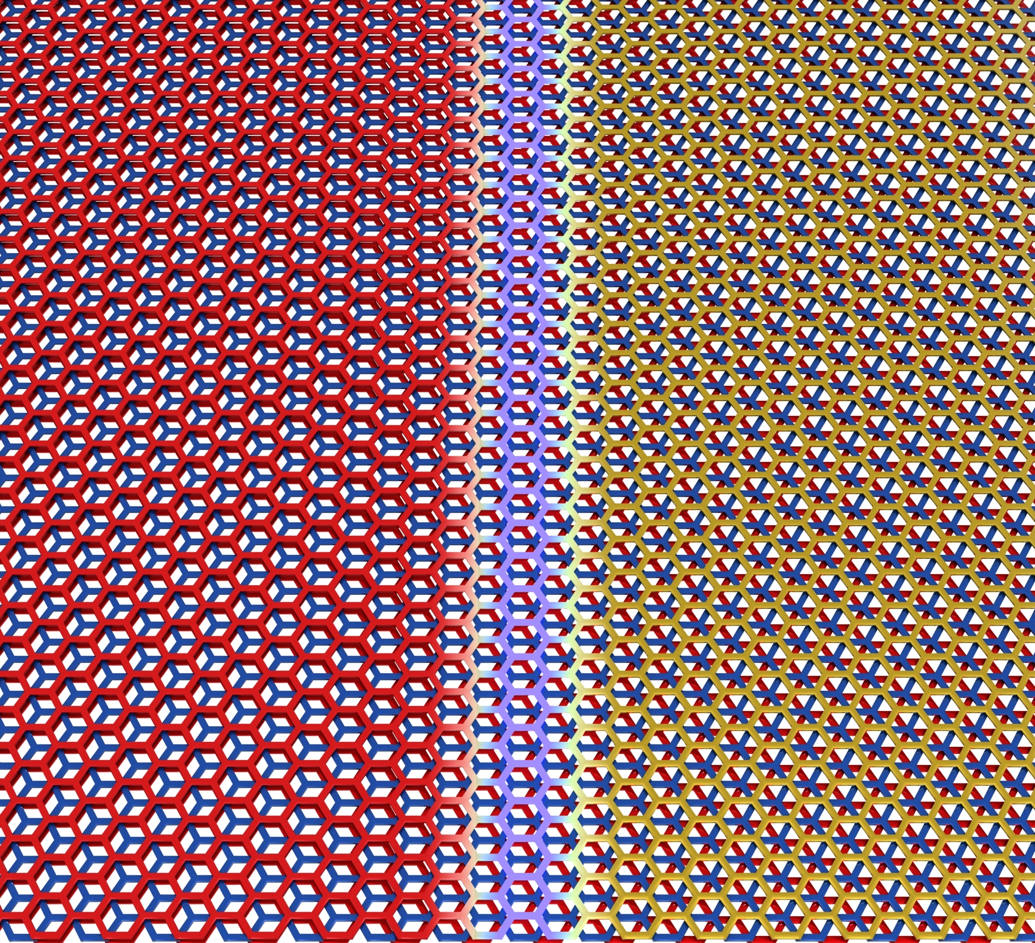
Graphene trilayers can be stacked in two different configurations, which can occur naturally in the same graphene flake. They are separated by a sharp boundary. (Credit: Pablo San-Jose ICMM-CSIC)
A University of Arizona-led team of physicists has discovered how to change the crystal structure of graphene with an electric field — a step toward the possible use of graphene in microprocessors that would be smaller and faster than current, silicon-based technology.
The tricky part is to control the flow of electrons through the material, a necessary prerequisite for using it an electronic circuit.
Brian LeRoy, UA associate professor of physics, and his collaborators have cleared a hurdle toward that goal by showing that an electric field is capable of controlling the crystal structure of trilayer graphene, transforming it from behaving as a metal to behaving as a semiconductor.

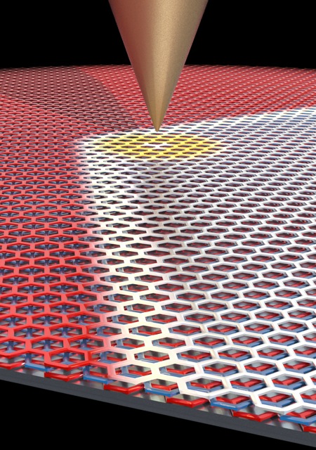
Using a sharp metal scanning tunneling microscopy tip, LeRoy and his collaborators were able to move the domain border between the two graphene configurations around (credit: Pablo San-Jose ICMM-CSIC)
Trilayer graphene can be stacked in two stacking configurations, which can naturally exist in the same flake of graphene. The two domains are separated by a sharp boundary where the carbon hexagons are strained to accommodate the transition from one stacking pattern to the other.
“Due to the different stacking configurations on either side of the domain wall, one side of the material behaves as a metal, while the other side behaves as a semiconductor,” LeRoy explained.
While probing the domain wall with an electric field, applied by an extremely sharp metal scanning tunneling microscopy tip, the researchers in LeRoy’s group discovered that they could move the position of the domain wall within the flake of graphene. And as they moved the domain wall, the crystal structure of the trilayer graphene changed in its wake.
By applying an electric field to move the boundary, it is now possible for the first time to change the crystal structure of graphene in a controlled fashion to create transistors from graphene.
Unlike silicon transistors used now, graphene-based transistors could be extremely thin, making the device much smaller, and since electrons move through graphene much faster than through silicon, the devices would enable faster computing.
In addition, silicon-based transistors function as one of two types — p-type or n-type — whereas graphene could operate as both. This would make them cheaper to produce and more versatile in their applications.
The study appears in Nature Materials.
“We expect this innovation could be used to create novel devices which combine both the structural and electronic properties of multilayer graphene,” Matthew Yankowitz, first author of the Nature Materials paper, explained to KurzweilAI in an email interview. “Most notably, the effect could be utilized to create a field effect transistor.”
However, he said considerable work is likely necessary before this effect can be utilized commercially. “While these domain walls between stacking configurations occur naturally in exfoliated graphene flakes, they can not yet be grown reliably using the industrially-scalable chemical vapor deposition method. Growth techniques are becoming steadily more sophisticated with time, and if this tricky problem can be solved, there is hope to utilize this effect commercially. First, more work must be done to create ‘proof-of-principle’ devices which operate with the desired properties.”
Researchers at MIT/Harvard University, U.S. Army Research Laboratory, National Institute for Materials Science (Japan), and Instituto de Ciencia de Materiales de Madrid were involved in the study.
Abstract of Nature Materials paper
The crystal structure of a material plays an important role in determining its electronic properties. Changing from one crystal structure to another involves a phase transition that is usually controlled by a state variable such as temperature or pressure. In the case of trilayer graphene, there are two common stacking configurations (Bernal and rhombohedral) that exhibit very different electronic properties. In graphene flakes with both stacking configurations, the region between them consists of a localized strain soliton where the carbon atoms of one graphene layer shift by the carbon–carbon bond distance. Here we show the ability to move this strain soliton with a perpendicular electric field and hence control the stacking configuration of trilayer graphene with only an external voltage. Moreover, we find that the free-energy difference between the two stacking configurations scales quadratically with electric field, and thus rhombohedral stacking is favoured as the electric field increases. This ability to control the stacking order in graphene opens the way to new devices that combine structural and electrical properties.
