Laser may replace copper in computer chips for high-speed, low-energy data transmission
January 22, 2015

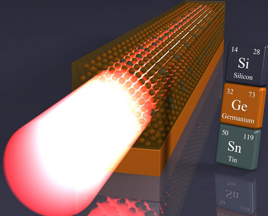
Schematic structure of the germanium-tin (GeSn) laser, applied directly onto the silicon wafer (blue) by using an intermediate layer of pure germanium (orange) (credit: Forschungszentrum Jülich)
An international team of scientists has constructed the first germanium-tin* semiconductor laser for CMOS silicon chips. By replacing copper wires with optical transmission, the new device promises higher-speed data transmission on computer chips at a fraction of the energy.
The results by scientists from Forschungszentrum Jülich and the Paul Scherrer Institute in Switzerland in cooperation with international partners were published in the journal Nature Photonics.
Transferring data between multiple cores and between logic elements and memory cells is a key bottleneck in fast-developing computer technology.
“Signal transmission via copper wires limits the development of larger and faster computers due to the thermal load and the limited bandwidth of copper wires,” explains Prof. Detlev Grützmacher, Director at the Forschungszentrum Jülich Peter Grünberg Institute. “The clock signal alone uses up to 30% of the energy, which can be saved through optical transmission.”
The more than 10% tin content is what enables the new germanium-tin semiconductor optical properties, according to the scientists.
The laser is currently limited to low temperatures of up to minus 183 degrees Celsius in the test system. The next big step will be generating laser light with electricity, and without the need for cooling, if possible. The aim is to create an electrically pumped laser that functions at room temperature.
*The basis of chip manufacturing is silicon, an element of main group IV of the periodic table. Typical semiconductor lasers for telecommunication systems, made of gallium arsenide for example, however, are costly and consist of elements from main groups III or V. This has profound consequences on the crystal properties.
Such laser components cannot therefore be applied directly onto silicon. They have to be produced externally at great effort and subsequently glued to the silicon wafer. However, the lifetime of this kind of component is greatly reduced due to the fact that the thermal expansion coefficients of these elements are significantly different from that of silicon.
In contrast, semiconductors of main group IV — to which both silicon and germanium belong — can be integrated into the manufacturing process without any major difficulties. Neither element by itself is very efficient as a light source, however. They are classed among the indirect semiconductors. In contrast to direct semiconductors, they emit mostly heat and only a little light when excited.
The scientists at Jülich’s Peter Grünberg Institute have now for the first time succeeded in creating a “real” direct main group IV semiconductor laser by combining germanium and tin, which is also classed in main group IV.
Abstract of Lasing in direct-bandgap GeSn alloy grown on Si
Large-scale optoelectronics integration is limited by the inability of Si to emit light efficiently, because Si and the chemically well-matched Ge are indirect-bandgap semiconductors. To overcome this drawback, several routes have been pursued, such as the all-optical Si Raman laser and the heterogeneous integration of direct-bandgap III–V lasers on Si. Here, we report lasing in a direct-bandgap group IV system created by alloying Ge with Sn without mechanically introducing strain. Strong enhancement of photoluminescence emerging from the direct transition with decreasing temperature is the signature of a fundamental direct-bandgap semiconductor. For T ≤ 90 K, the observation of a threshold in emitted intensity with increasing incident optical power, together with strong linewidth narrowing and a consistent longitudinal cavity mode pattern, highlight unambiguous laser action. Direct-bandgap group IV materials may thus represent a pathway towards the monolithic integration of Si-photonic circuitry and complementary metal–oxide–semiconductor (CMOS) technology.
