Nanoscale optical switch breaks miniaturization barrier
March 18, 2014

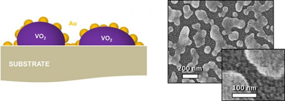
Left: Illustration of terahertz optical switches shows the vanadium dioxide nanoparticles (purple) coated with a “nanomesh” (yellow) of smaller gold particles. Right: Scanning electron microscope image of the switches at two resolutions. (Credit: Haglund Lab / Vanderbilt)
A new ultra-fast, ultra-small optical switch could advance the day when photons replace electrons in consumer products ranging from cell phones to automobiles. It was developed by a team of scientists from Vanderbilt University, University of Alabama-Birmingham, and Los Alamos National Laboratory.
Described in the March 12 issue of the journal Nano Letters, the new optical device can turn on and off trillions of times per second. It consists of individual switches that are only 200 nanometers in diameter — much smaller than the current generation of optical switches. It overcomes one of the major technical barriers to the spread of electronic devices that detect and control light: miniaturizing the size of ultrafast optical switches.
Gold nanoparticles use as small of one-tenth as much energy
The ultrafast switch is made out of a metamaterial (artificial material) engineered to have properties that are not found in nature. The metamaterial consists of nanoscale particles of vanadium dioxide (VO2) — a crystalline solid that can rapidly switch back and forth between an opaque, metallic phase and a transparent, semiconducting phase — which are deposited on a glass substrate and coated with a “nanomesh” of tiny gold nanoparticles.
The scientists report that bathing these gold nanoparticles with brief pulses from an ultrafast laser generates hot electrons in the gold particles that jump into the vanadium dioxide and cause it to undergo its phase change in a few trillionths of a second.
“We had previously triggered this transition in vanadium dioxide nanoparticles directly with lasers and we wanted to see if we could do it with electrons as well,” said Richard Haglund, Stevenson Professor of Physics at Vanderbilt, who led the study. “Not only does it work, but the injection of hot electrons from the gold nanoparticles also triggers the transformation with one fifth to one tenth as much energy input required by shining the laser directly on the bare VO2.”
Both industry and government are investing heavily in efforts to integrate optics and electronics, because it is generally considered to be the next step in the evolution of information and communications technology. Intel, Hewlett-Packard and IBM have been building chips with increasing optical functionality for the last five years that operate at gigahertz speeds, one thousandth that of the VO2 switch.
Ideal for optoelectronics
“Vanadium dioxide switches have a number of characteristics that make them ideal for optoelectronics applications,” said Haglund. In addition to their fast speed and small size, they:
- Are completely compatible with current integrated circuit technology, both silicon-based chips and the new “high-K dielectric” materials that the semiconductor industry is developing to continue the miniaturization process that has been a major aspect of microelectronics technology development;
- Operate in the visible and near-infrared region of the spectrum that is optimal for telecommunications applications;
- Generate an amount of heat per operation that is low enough so that the switches can be packed tightly enough to make practical devices: about ten trillionths of a calorie (100 femtojoules) per bit.
“Vanadium dioxide’s amazing properties have been known for more than half a century. At Vanderbilt, we have been studying VO2 nanoparticles for the last ten years, but the material has been remarkably successfully at resisting theoretical explanations,” said Haglund. “It is only in the last few years that intensive computational studies have illuminated the physics that underlies its semiconductor-to-metal transition.”
The university researchers were supported by Defense Threat-Reduction Agency grant HDTRA1-0047, U.S. Department of Energy grant DE-FG02-01ER45916, U.S. Department of Education GAANN Fellowship P200A090143 and National Science Foundation grant DMR-1207241.
Abstract of Nano Letters paper
Ultrafast photoinduced phase transitions could revolutionize data-storage and telecommunications technologies by modulating signals in integrated nanocircuits at terahertz speeds. In quantum phase-changing materials (PCMs), microscopic charge, lattice, and orbital degrees of freedom interact cooperatively to modify macroscopic electrical and optical properties. Although these interactions are well documented for bulk single crystals and thin films, little is known about the ultrafast dynamics of nanostructured PCMs when interfaced to another class of materials as in this case to active plasmonic elements. Here, we demonstrate how a mesh of gold nanoparticles, acting as a plasmonic photocathode, induces an ultrafast phase transition in nanostructured vanadium dioxide (VO2) when illuminated by a spectrally resonant femtosecond laser pulse. Hot electrons created by optical excitation of the surface-plasmon resonance in the gold nanomesh are injected ballistically across the Au/VO2 interface to induce a subpicosecond phase transformation in VO2. Density functional calculations show that a critical density of injected electrons leads to a catastrophic collapse of the 6 THz phonon mode, which has been linked in different experiments to VO2 phase transition. The demonstration of subpicosecond phase transformations that are triggered by optically induced electron injection opens the possibility of designing hybrid nanostructures with unique nonequilibrium properties as a critical step for all-optical nanophotonic devices with optimizable switching thresholds.
