New form of graphene allows electrons to behave like photons
February 6, 2014

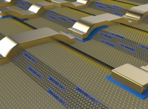
This is a conceptual drawing of an electronic circuit comprised of interconnected graphene nanoribbons (black atoms) that are epitaxially grown on steps etched in silicon carbide (yellow atoms). Electrons (blue) travel ballistically along the ribbon and then from one ribbon to the next via the metal contacts. Electron flow is modulated by electrostatic gates. (Credit: John Hankinson)
Using electrons more like photons could provide the foundation for a new type of electronic device that would capitalize on the ability of graphene to carry electrons with almost no resistance even at room temperature — a property known as ballistic transport.
Research reported this week in the journal Nature shows that electrical resistance in nanoribbons of epitaxial graphene changes in discrete steps following quantum mechanical principles. The research shows that the graphene nanoribbons act more like optical waveguides or quantum dots, allowing electrons to flow smoothly along the edges of the material.
In ordinary conductors such as copper, resistance increases in proportion to the length as electrons encounter more and more impurities while moving through the conductor.
Over ten times more conductive
The ballistic transport properties, similar to those observed in cylindrical carbon nanotubes, exceed theoretical conductance predictions for graphene by a factor of 10. The properties were measured in graphene nanoribbons approximately 40 nanometers wide that had been grown on the edges of three-dimensional structures etched into silicon carbide wafers.
“This work shows that we can control graphene electrons in very different ways because the properties are really exceptional,” said Walt de Heer, a Regent’s professor in the School of Physics at the Georgia Institute of Technology. “This could result in a new class of coherent electronic devices based on room temperature ballistic transport in graphene. Such devices would be very different from what we make today in silicon.”
The research, which was supported by the National Science Foundation, the Air Force Office of Scientific Research and the W.M. Keck Foundation, was done through a collaboration of scientists from Georgia Tech in the U.S., Leibniz Universität Hannover in Germany, the Centre National de la Recherche Scientifique (CNRS) in France, and Oak Ridge National Laboratory in the U.S.
Ultra-fast computing with graphene
For nearly a decade, researchers have been trying to use the unique properties of graphene to create electronic devices that operate much like existing silicon semiconductor chips. But those efforts have met with limited success because graphene cannot be easily given the electronic bandgap that such devices need to operate.
De Heer argues that researchers should stop trying to use graphene like silicon, and instead use its unique electron transport properties to design new types of electronic devices that could allow ultra-fast computing — based on a new approach to switching. Electrons in the graphene nanoribbons can move tens or hundreds of microns without scattering.
“This constant resistance is related to one of the fundamental constants of physics, the conductance quantum,” de Heer said. “The resistance of this channel does not depend on temperature, and it does not depend on the amount of current you are putting through it.”
Nanoribbons of epitaxial graphene

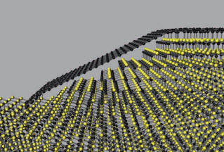
Schematic showing well-aligned, single-crystal monolayer graphene sheets (all black) that form spontaneously on steps etched onto the surface of silicon carbide (SiC) wafers heated above 1,000 degrees C (credit: Jens Baringhaus et al./Nature)
The nanoribbons are grown epitaxially on silicon carbide (SiC) wafers into which patterns have been etched using standard microelectronics fabrication techniques.
When the wafers are heated to approximately 1,000 degrees Celsius, silicon is preferentially driven off along the edges, forming graphene nanoribbons whose structure is determined by the pattern of the three-dimensional surface.
Once grown, the nanoribbons require no further processing.
The advantage of fabricating graphene nanoribbons this way is that it produces edges that are perfectly smooth, annealed by the fabrication process.
Electrons that behave like photons
The smooth edges allow electrons to flow through the nanoribbons without disruption. (If traditional etching techniques are used to cut nanoribbons from graphene sheets, the resulting edges are too rough to allow ballistic transport.)
“It seems that the current is primarily flowing on the edges,” de Heer said. “There are other electrons in the bulk portion of the nanoribbons, but they do not interact with the electrons flowing at the edges.”
The electrons on the edge flow more like photons in optical fiber, helping them avoid scattering. “These electrons are really behaving more like light,” he said. “It is like light going through an optical fiber. Because of the way the fiber is made, the light transmits without scattering.”
The researchers measured ballistic conductance in the graphene nanoribbons for up to 16 microns. Electron mobility measurements surpassing one million correspond to a sheet resistance of one ohm per square that is two orders of magnitude lower than what is observed in two-dimensional graphene — and ten times smaller than the best theoretical predictions for graphene.

Walt de Heer, a Regent’s professor in the School of Physics at the Georgia Institute of Technology, with equipment used to measure the properties of graphene nanoribbons (credit: Georgia Tech/Rob Felt)
A new type of graphene-based electronics
“This should enable a new way of doing electronics,” de Heer said. “We are already able to steer these electrons and we can switch them using rudimentary means. We can put a roadblock, and then open it up again. New kinds of switches for this material are now on the horizon.”
Theoretical explanations for what the researchers have measured are incomplete. De Heer speculates that the graphene nanoribbons may be producing a new type of electronic transport similar to what is observed in superconductors.
“There is a lot of fundamental physics that needs to be done to understand what we are seeing,” he added. “We believe this shows that there is a real possibility for a new type of graphene-based electronics.”
Georgia Tech researchers have pioneered graphene-based electronics since 2001, for which they hold a patent, filed in 2003. The technique involves etching patterns into electronics-grade silicon carbide wafers, then heating the wafers to drive off silicon, leaving patterns of graphene.
This research was supported by the National Science Foundation (NSF) Materials Research Science and Engineering Center (MRSEC) at Georgia Tech; the Air Force Office of Scientific Research (AFOSR); the Scientific User Facilities Division, Office of Basic Energy Sciences, U.S. Department of Energy, and the Partner University Fund from the Embassy of France.
Abstract of Nature paper
Graphene nanoribbons will be essential components in future graphene nanoelectronics. However, in typical nanoribbons produced from lithographically patterned exfoliated graphene, the charge carriers travel only about ten nanometres between scattering events, resulting in minimum sheet resistances of about one kilohm per square. Here we show that 40-nanometre-wide graphene nanoribbons epitaxially grown on silicon carbide are single-channel room-temperature ballistic conductors on a length scale greater than ten micrometres, which is similar to the performance of metallic carbon nanotubes. This is equivalent to sheet resistances below 1 ohm per square, surpassing theoretical predictions for perfect graphene by at least an order of magnitude. In neutral graphene ribbons, we show that transport is dominated by two modes. One is ballistic and temperature independent; the other is thermally activated. Transport is protected from back-scattering, possibly reflecting ground-state properties of neutral graphene. At room temperature, the resistance of both modes is found to increase abruptly at a particular length—the ballistic mode at 16 micrometres and the other at 160 nanometres. Our epitaxial graphene nanoribbons will be important not only in fundamental science, but also – because they can be readily produced in thousands – in advanced nanoelectronics, which can make use of their room-temperature ballistic transport properties.
