Next-generation energy-efficient light-based computers
June 4, 2015

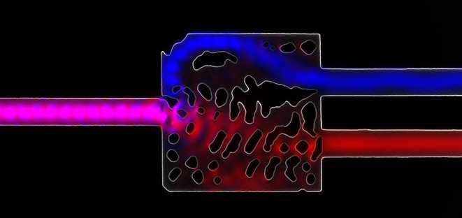
Infrared light enters this silicon structure from the left. The cut-out patterns, determined by an algorithm, route two different wavelengths of this light into the two pathways on the right. (credit: Alexander Piggott)
Stanford University engineers have developed a new design algorithm that can automate the process of designing optical interconnects, which could lead to faster, more energy-efficient computers that use light rather than electricity for internal data transport.
Light can transmit more data while consuming far less power than electricity. According to a study by David Miller, the MIT W.M. Keck Foundation Professor of Electrical Engineering, up to 80 percent of microprocessor power is consumed by sending data over interconnects (wires that connect chips).
In addition, “for chip-scale links, light can carry more than 20 times as much data,” said Stanford graduate student Alexander Y. Piggott, lead author of a Nature Photonics article.
However, designing optical interconnects (using silicon fiber-optics cables) is complex and requires custom design for each interconnect. Given that thousands of interconnects are needed for each electronic system, optical data transport has remained impractical.
Optimized design of optical interconnects
Now the Stanford engineers believe they’ve broken that bottleneck by inventing what they call an “inverse design algorithm.” It works as the name suggests: the engineers specify what they want the optical circuit to do, and the software provides the details of how to fabricate a silicon structure to perform the task.

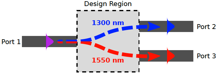
The wavelength demultiplexer developed by the Stanford team comprised one input waveguide, two output waveguides, and a chip for switching outputs based on incoming wavelengths (credit: Alexander Y. Piggott et al./Nature Photonics)
“We used the algorithm to design a working optical circuit and made several copies in our lab,” said Jelena Vuckovic, a Stanford professor of electrical engineering and senior author of the article.
The optical circuit they created was a silicon wavelength demultiplexer (which splits incoming light into multiple channels based on the wavelengths of the light). The device split 1,300 nm and 1,550 nm light from an input waveguide into two output waveguides.
(“Multiplexing” allows for multiple signals to be transmitted over a thin fiber-optic cable, which is how the Internet and cable television is able to transmit massive amounts of data, not possible with wires.)
The engineers note that once the algorithm has calculated the proper shape for the task, standard scalable industrial processes can be used to transfer that pattern onto silicon. The device footprint is only 2.8 x 2.8 micrometers, making this the smallest dielectric wavelength splitter to date.
The researchers envision other potential applications for their inverse design algorithm, including high-bandwidth optical communications, compact microscopy systems, and ultra-secure quantum communications.
Abstract of Inverse design and demonstration of a compact and broadband on-chip wavelength demultiplexer
Integrated photonic devices are poised to play a key role in a wide variety of applications, ranging from optical interconnects and sensors to quantum computing. However, only a small library of semi-analytically designed devices is currently known. Here, we demonstrate the use of an inverse design method that explores the full design space of fabricable devices and allows us to design devices with previously unattainable functionality, higher performance and robustness, and smaller footprints than conventional devices. We have designed a silicon wavelength demultiplexer that splits 1,300 nm and 1,550 nm light from an input waveguide into two output waveguides, and fabricated and characterized several devices. The devices display low insertion loss (∼2 dB), low crosstalk (<−11 dB) and wide bandwidths (>100 nm). The device footprint is 2.8 × 2.8 μm2, making this the smallest dielectric wavelength splitter.
