One-atom-thin ‘silicene’ silicon transistors invented
February 5, 2015

Buckled honeycomb lattice structure of silicene (credit: Li Tao et al./Nature Nanotechnology)
The first transistors made of silicene, the world’s thinnest silicon material, have been developed by researchers at The University of Texas at Austin’s Cockrell School of Engineering. The new material may allow for building dramatically faster, smaller, energy-efficient computer chips.
Made of a one-atom-thick layer of silicon atoms, silicene has outstanding electrical properties but has until now proved difficult to produce and work with.
Deji Akinwande, an assistant professor in the Cockrell School’s Department of Electrical and Computer Engineering, and his team, including lead researcher Li Tao, solved one of the major challenges surrounding silicene by demonstrating that it can be made into transistors.
Thinnest semiconductor material
These first-of-their-kind devices rely on the thinnest of any semiconductor material, a long-standing dream of the chip industry. Their work was published this week in the journal Nature Nanotechnology.

In situ scanning tunneling microscopy (STM) shows three main silicon overlayers (credit: Li Tao et al./Nature Nanotechnology)
Until a few years ago, human-made silicene was a purely theoretical material. Looking at carbon-based graphene, another atom-thick material with promise for chip development, researchers speculated that silicon atoms could be structured in a broadly similar way.
“Silicene, with its close chemical affinity to silicon, suggests an opportunity in the roadmap of the semiconductor industry,” Akinwande said. “The major breakthrough here is the efficient low-temperature manufacturing and fabrication of silicene devices for the first time.”
Despite its promise for commercial adaptation, silicene has proved extremely difficult to create and work with because of its complexity and instability when exposed to air.
How to fabricate silicene
To work around these issues, Akinwande teamed with Alessandro Molle at the Institute for Microelectronics and Microsystems in Agrate Brianza, Italy, to develop a new method for fabricating the silicene that reduces its exposure to air.

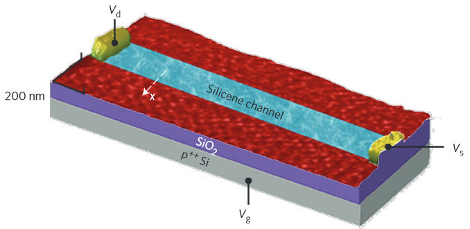
Three-dimensional rendering of AFM image on a silicene field effect transistor on 90-nm-thick silicon dioxide/silicon substrate, including the channel and source (Vs)/drain (Vd) contacts (credit: Li Tao et al./Nature Nanotechnology)
To start, the researchers let a hot vapor of silicon atoms condense onto a crystalline block of silver in a vacuum chamber. They then formed a silicene sheet on a thin layer of silver and added a nanometer-thick layer of alumina on top. Because of these protective layers, the team could safely peel it of its base and transfer it silver-side-up to an oxidized-silicon substrate. They were then able to gently scrape some of the silver to leave behind two islands of metal as electrodes, with a strip of silicene between them.
In the near-term, Akinwande will continue to investigate new structures and methods for creating silicene, which may lead to low-energy, high-speed digital computer chips.
The U.S. Army Research Laboratory’s Army Research Office, the Cockrell School’s Southwest Academy of Nanoelectronics and the European Commission’s Future and Emerging Technologies Programme funded Akinwande’s research.
Abstract of Silicene field-effect transistors operating at room temperature
Free-standing silicene, a silicon analogue of graphene, has a buckled honeycomb lattice and, because of its Dirac bandstructurecombined with its sensitive surface, offers the potential for a widely tunable two-dimensional monolayer, where external fields and interface interactions can be exploited to influence fundamental properties such as bandgap and band characterfor future nanoelectronic devices. The quantum spin Hall effect, chiral superconductivity, giant magnetoresistance and various exotic field-dependent states have been predicted in monolayer silicene. Despite recent progress regarding the epitaxial synthesis of silicene and investigation of its electronic properties, to date there has been no report of experimental silicene devices because of its air stability issue. Here, we report a silicene field-effect transistor, corroborating theoretical expectations regarding its ambipolar Dirac charge transport, with a measured room-temperature mobility of ∼100 cm2 V–1 s–1 attributed to acoustic phonon-limited transport and grain boundary scattering. These results are enabled by a growth–transfer–fabrication process that we have devised—silicene encapsulated delamination with native electrodes. This approach addresses a major challenge for material preservation of silicene during transfer and device fabrication and is applicable to other air-sensitive two-dimensional materials such as germanene and phosphorene. Silicene’s allotropic affinity with bulk silicon and its low-temperature synthesis compared with graphene or alternative two-dimensional semiconductors suggest a more direct integration with ubiquitous semiconductor technology.
