Replacing wires with light, future computers may operate faster with less energy
December 2, 2014

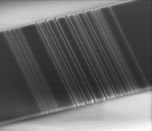
This tiny slice of silicon, etched with a grating pattern that resembles a bar code, is a key step toward linking computer components with light instead of wires (credit: Vuckovic Lab)
Stanford engineers have designed and built a prism-like silicon device that can split a beam of light into different colors and bend the light at right angles — a development that could eventually lead to computers that use nanophotonics to transmit data faster and more efficiently than electricity.
They describe this “optical link” —a tiny slice of silicon etched with a pattern that resembles a bar code — in an article in Scientific Reports (open access).
When a beam of light shines at the silicon device, two different wavelengths (colors) of light split off at right angles to the input, forming a T shape.
“Light can carry more data than a wire, and it takes less energy to transmit photons than electrons,” said electrical engineering Professor Jelena Vuckovic, who led the research.
In previous work, her team developed an algorithm that automated the process of designing optical structures and enabled the researchers to create previously unimaginable nanoscale structures to control light.
Now, she and lead author Alexander Piggott, a doctoral candidate in electrical engineering, have employed that algorithm to design, build, and test an optical-link device that is compatible with current fiber optic networks.
Creating a silicon prism
The new device was made by etching a tiny bar-code-like pattern into silicon. The pattern splits light, similar to how a prism works.
The Stanford algorithm designed a structure that alternated strips of silicon and gaps of air in a specific way. The device takes advantage of the fact that as light passes from one medium to the next, some light is reflected and some is transmitted. When light traveled through the silicon bar code, the reflected light interfered with the transmitted light in complicated ways, depending on the based on the material’s index of refraction*.
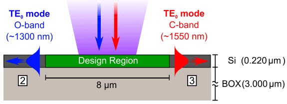
The algorithm designed the bar code to use this subtle interference to direct one wavelength to go left and a different wavelength to go right, all within a tiny silicon chip eight micrometers (millionths of a meter) long.

The optical-link device is fabricated by etching a 220 nm silicon layer on 3 mm of buried oxide, in the pattern produced by the optimization algorithm; when 1300 nm infrared light hits the material, it is refracted left, while 1550 nm light is refracted right (the colors are for illustration only) (credit: Vuckovic Lab)
Both 1300-nanometer light and 1550-nanometer light, corresponding to C-band and O-band wavelengths widely used in fiber optic networks, were beamed at the device from above. The bar code-like structure redirected C-band light one way and O-band light the other, right on the chip.
A major design improvement
“For many years, nanophotonics researchers made structures using simple geometries and regular shapes,” Vuckovic said. “The structures you see produced by this algorithm are nothing like what anyone has done before.”
The algorithm began its work with a simple design of just silicon. Then, through hundreds of tiny adjustments, it found better and better bar code structures for producing the desired output light.
Previous designs of nanophotonic structures were based on regular geometric patterns and the designer’s intuition, a time-consuming process. The Stanford algorithm can now design this structure in just 15 minutes on a laptop computer.
The Stanford researchers have also used this algorithm to design a wide variety of other devices, like the super-compact “Swiss cheese” structures that route light beams to different outputs not based on their color, but based on their mode, i.e., based on how they look. For example, a light beam with a single lobe in the cross-section goes to one output, and a double lobed beam (looking like two rivers flowing side by side) goes to the other output. Such a mode router is equally as important as the bar code color splitter, as different modes are also used in optical communications to transmit information.
* The conventional “speed of light” (about 300 million meter per second) is how fast light travels in a vacuum. However, light actually travels a bit more slowly in air and even more slowly in water. This speed difference is why a straw in a glass of water looks dislocated. A property of materials called the index of refraction characterizes the difference in speed. The higher the index, the more slowly light will travel in that material. Air has an index of refraction of nearly 1 and water of 1.3. Infrared light travels through silicon even more slowly: it has an index of refraction of 3.5
Abstract of Inverse design and implementation of a wavelength demultiplexing grating coupler
Nanophotonics has emerged as a powerful tool for manipulating light on chips. Almost all of today’s devices,
however, have been designed using slow and ineffective brute-force search methods, leading in many cases to
limited device performance. In this article, we provide a complete demonstration of our recently proposed
inverse design technique, wherein the user specifies design constraints in the form of target fields rather
than a dielectric constant profile, and in particular we use this method to demonstrate a new demultiplexing
grating. The novel grating, which has not been developed using conventional techniques, accepts a
vertical-incident Gaussian beam from a free-space and separates O-band (1300 nm) and C-band (1550 nm)
light into separate waveguides. This inverse design concept is simple and extendable to a broad class of
highly compact devices including frequency filters, mode converters, and spatial mode multiplexers.
