Ultrasonic waves allow for precision micro- and nano-manufacturing of thin-film chips
June 27, 2014

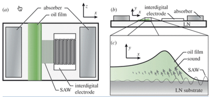
An oil strip is deposited on the piezoelectric substrate along a line perpendicular to the surface acoustic wave (SAW) propagation path, as shown in (a) the top and (b) the side. Gel absorbers, placed at either end of the device, absorb the SAW generated by the interdigital electrode, preventing edge reflections and ensuring (c) the deformation of the film is as a result of pure SAWs. (Credit: Amgad R. Rezk et al./Proceedings of the Royal Society A)
Researchers at RMIT University in Melbourne, Australia, have developed a method for using ultrasonics to enable precision micro- and nano-manufacturing, precisely controlling the spread of a thin-film fluid along a specially designed chip.
Thin-film technology is the bedrock of microchip and microstructure manufacturing, and applications of the research range from thin-film coatings for paint and wound care to 3D printing, micro-casting, and micro-fluidics.
“Manufacturing using thin film technology currently lacks precision — structures are physically spun around to disperse the liquid and coat components with thin film, explained Professor James Friend, Director of the MicroNano Research Facility at RMIT.
“We’ve found that thin-film liquid either flows towards or away from high-frequency sound waves, depending on its thickness. By tuning the sound waves, we can create any pattern we want on the surface of a microchip.”
Friend said the researchers have also unraveled the complex physics behind the process, enabling them to “precisely control and direct the application of thin-film liquid at a micro and nano-scale.”
The new “acoustowetting” process was shown to work on a chip made of lithium niobate — a piezoelectric material capable of converting electrical energy into mechanical pressure.
The surface of the chip is covered with microelectrodes and the chip is connected to source of ultrasonic waves (10 to 1,000 MHz). Thin-film liquid is added to the surface of the chip, and the “surface acoustic waves” are then used to control its flow.
The research shows that when the liquid is ultra-thin — at nano and sub-micro depths — it flows away from the high-frequency sound waves. The flow reverses at slightly thicker dimensions, moving towards the sound waves. But at a millimeter or more in depth, the flow reverses again, moving away.
The research is described in a paper published in Proceedings of the Royal Society A (open access).
RMIT University researchers have harnessed the power of soundwaves to enable precision micro- and nano-manufacturing. The researchers have demonstrated how high-frequency soundwaves can be used to precisely control the spread of thin film fluid along a specially-designed chip. This video shows the behavior of a drop of fluorescent silicon oil when struck with high frequency sound waves at 30MHz (magnification x30). The new process, which the team call “acoustowetting”, works on a chip made of lithium niobate – a piezoelectric material capable of converting electrical energy into mechanical pressure. The surface of the chip is covered with microelectrodes and the chip is connected to a power source, with the power converted to high-frequency soundwaves. Thin film liquid is added to the surface of the chip, and the soundwaves are then used to control its flow. The research shows that when the liquid is ultra-thin –\ at nano and sub-micro depths — it flows away from the high-frequency sound waves. The flow reverses at slightly thicker dimensions, moving towards the sound waves. But at a millimetre or more in depth, the flow reverses again, moving away.
Abstract of Proceedings of the Royal Society A paper
Arising from an interplay between capillary, acoustic and intermolecular forces, surface acoustic waves (SAWs) are observed to drive a unique and curious double flow reversal in the spreading of thin films. With a thickness at or less than the submicrometre viscous penetration depth, the film is seen to advance along the SAW propagation direction, and self-similarly over time t1/4 in the inertial limit. At intermediate film thicknesses, beyond one-fourth the sound wavelength λℓ in the liquid, the spreading direction reverses, and the film propagates against the direction of the SAW propagation. The film reverses yet again, once its depth is further increased beyond one SAW wavelength. An unstable thickness region, between λℓ/8 and λℓ/4, exists from which regions of the film either rapidly grow in thickness to exceed λℓ/4 and move against the SAW propagation, consistent with the intermediate thickness films, whereas other regions decrease in thickness below λℓ/8 to conserve mass and move along the SAW propagation direction, consistent with the thin submicrometre films.
